By John McHale
The methods for making processors and integrated circuits (ICs) radiation hardened (rad-hard) have not changed much, but the chips themselves are getting smaller, faster, and generating more heat than ever before.
“When we focus on processors it is on the processor suite” and its elements, says Vic Scuderi, manager of satellite electronics for BAE Systems in Manassas, Va. Right now, U.S. Department of Defense (DOD) users focus on horsepower, or number of instructions per second the microprocessor can handle, he adds.
The RAD750 processor from BAE Systems clocks in with as much as 260 million instructions per second (MIPS), Scuderi says. These speeds create heat–and present thermal and power challenges, he adds.
“In space, it is difficult to cool processors and supply power,” says Keith Nootbaar, senior director for microelectronics and precision sensors at Honeywell Aerospace in Plymouth, Minn. Designers are “asking not about performance, but about the power and performance ratio,” he continues.
Users are able to manage the MIPS rate through software, depending on the power requirements of their applications, Scuderi says. “It enables them to dial down the MIPS,” he says.
Honeywell also enables designers to manage their clock rate, Nootbaar says. Each of the company’s RHPPC 603e processors has three different clock settings, he adds. The 603e is based on PowerPC technology from Freescale Semiconductor and “from a total dose standpoint its immunity is greater than 1 megarad,” Nootbaar notes.
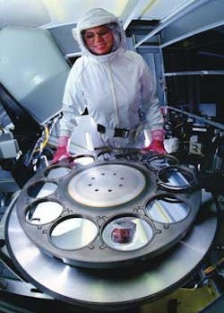
A technician in the Microelectronics Development Laboratory at Sandia National Laboratories works with one of several metal deposition systems used for radiation-hardened microelectronics processing.
Space designers demand that type of functionality Scuderi says. It is part of a low-power strategy for electronics, he adds. Later this year, a version of the RAD750 will range from 400 to 500 MIPS and be hardened to one megarad, Scuderi continues.
BAE Systems and Honeywell do radiation hardening by process, which provides much greater radiation protection than the hardening by design methods that commercial foundries use, Nootbaar says. Rad hard by process results in zero latchups, he adds.
“We use silicon on insulator,” which provides 10 times the single event upset (SEU) performance of bulk silicon, Nootbaar says. Also, in lower earth orbit, there is a need for heavy proton immunity, and ICs from commercial foundries are more susceptible to proton upsets, he adds.
Another reason the DOD community is moving away from commercial foundries involves the large number of offshore foundries, which DOD leaders see as security risks, Nootbaar says. “There is a concern that with offshore production, there could be “intrusions into the circuitry,” he explains.
The DOD created the Trusted Foundry program to deal with potential risks–including design tampering–that may occur in offshore facilities.
Looking toward the future, Scuderi predicts that the sizes of ICs will continue to get smaller. Currently, “we are at 0.15 nanometers,” he says.
The smaller sizes bring benefits, but also “challenges because as sizes shrink, SEUs, heavy ions, and solar flares” will have a much bigger effect on the chips, Scuderi continues. He declined to go into specifics on how he and his colleagues will attack that challenge.
As for five or 10 years down the road, Honeywell’s Nootbaar says he sees carbon nanotubes as the next technological game changer. The molecular design would create ICs that are high-speed, low-power, and inherently rad-hard, Nootbaar says.
“Radiation does not affect the molecular structure,” Nootbaar adds, predicting that carbon nanotube memory will be a reality in roughly five years, and rad-hard processors in about 10.

