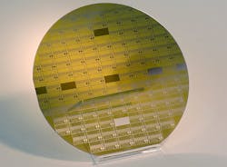
Air Force eyes program to develop silicon carbide films for radar and EW semiconductor wafers
WRIGHT-PATTERSON AFB, Ohio, 9 Aug. 2016. U.S. Air Force researchers will announce a project next month to stand-up a manufacturer of affordable high quality silicon carbidefilms for RF and power switching semiconductor wafers for radar, electronic warfare (EW), and military communications.
Officials of the Air Force Research Laboratory at Wright-Patterson Air Force Base, Ohio, issued a presolicitation (FA8650-16-S-1727) on Friday for the Development of Large-Diameter Silicon Carbide Substrates and Homoepitaxial Processes project.
This initiative seeks to find a qualified manufacturer able to fabricate conducting (4H N-doped) and semi-insulating (6H V-doped) silicon carbide substrates and epitaxial films for advanced gallium nitride and silicon carbide RF and power switching semiconductors.
Such technology is expected to be crucial to Air Force sensor superiority for radar, EW, and communications in the DC to microwave and submillimeter-wave spectrum from 300 MHz to 300 GHz, researchers say.
Using homo/hetero-epitaxial devices fabricated on silicon carbide holds promise for revolutionary improvements in the cost, size, weight, and performance of a broad range of military RF, power-management, and power-distribution components, experts say.
Related: Army research eyes next-generation SiC military high-voltage switching devices
Gallium nitride high electron mobility transistors (HEMTs) rapidly are becoming the technology of choice for high-power RF amplification. The combination of high voltage and current handling as well as switching frequency capabilities make silicon carbide power devices a viable alternative to silicon technology.
Fabrication of silicon carbide power devices requires homo-epitaxial growth of precisely doped silicon carbide layers ranging in thickness from a few microns to more than 100 microns. The availability of large-diameter semiconducting and semi-insulating silicon carbide substrates will be crucial to fabricating these kinds of devices, researchers say.
This project involves development, assessment, and manufacturing of single-crystal silicon carbide boules, homoepitaxial films, and related device demonstrations. technical goals include silicon carbide crystal growth; substrate fabrication and polishing; homoepitaxy; material characterization; and material and device correlation.
Air Force officials say they plan to release a former solicitation for the Development of Large-Diameter Silicon Carbide Substrates and Homoepitaxial Processes project in September 2016.
The project should be worth $13.1 million -- of which $11.2 million will come from the government. Air Force researchers say they expect the winning contractor to invest about $1.7 million in the project.
Email technical questions or concerns to Project Engineer John Blevins by email at [email protected]. Email contracting questions to Contract Specialist Joe Strehle at joseph.strehle @us.af.mil.
More information is online at https://www.fbo.gov/spg/USAF/AFMC/AFRLWRS/FA8650-16-S-1727/listing.html.
Learn more: search the Aerospace & Defense Buyer's Guide for companies, new products, press releases, and videos

