Planar lightwave circuits will be a key technology for next-generation military systems
By Rick Stevens and Joseph Shmulovich
In the mid-1960s, U.S. missile-defense capability and the electronics industry took off together. Designers of the Minuteman II missile found their conventional guidance and control systems - made from a collection of discrete electronic components - too heavy, too bulky to fit, and too unreliable for accurate intercontinental targeting. The challenges posed by that era’s geopolitical threats required a much better technological response. Missile designers answered with integrated electronics.
The result: several functions combined seamlessly into one integrated circuit (IC) - one of the major innovations of the 20th century - and a new generation of Minuteman missiles that, with steady refinement, survives to this day. As for commercial electronics, the initial boost from defense helped that crucial industry mature much more quickly than it would have otherwise.
Today, some 40 years later, we find ourselves on the verge of a similar joint military/industrial breakthrough: integration of optoelectronics. Optoelectronics, or photonics, is now becoming crucial to communications systems on a variety of military platforms and sensor applications.
As in almost every significant technological transformation, the driving forces are multilayered and complex. The rise of diffuse and unpredictable terrorist and guerilla tactics on the battlefield and at home necessitates much faster, more nuanced responses. We need to know where a more mobile, more easily camouflaged enemy is, we need to know what he is targeting, and we need to know what weapons he is using.
Global positioning, weather information at the microclimate level, motion detection for everything from individual combatants to oncoming missiles, and chemical and bacteriological identification, and so on - all have suddenly become essential data for effective combat. All that data requires orders-of-magnitude more processing and higher bandwidth links as our land, sea, and air platforms grow smarter and more dependent on the integrated information suite delivered by the multitude of sensors.
The performance and scalability requirements of modern weapon platforms are such that the weight and volume associated with the communication system is becoming prohibitively large for virtually every platform, including unmanned aerial vehicles (UAVs), helicopters, fighter planes, tanks, submarines, or even surface ships. Not only do those requirements apply to new platforms, they also apply to older platforms that must be upgraded to process all the new information.
Photonics has the potential to fill all these military needs and more.
Fiber carries orders of magnitude more data - gigabits instead of kilobits. Fiber cable is significantly lighter than copper cable because it doesn’t require electromagnetic-interference (EMI) protective metal shielding and occupies much less space; think of all those heavy radar RF cables winding through airplanes and ships.
Unlike copper, fiber is scalable. Try upgrading a UAV with copper cables that already have been designed for a given frequency.
Photonics is relatively immune to EMI and electromagnetic pulse (EMP) weaponry; an enemy with high-energy weapons is much less likely to disturb fiber-based platforms.
Finally, fiber is nonconductive and therefore does not arc or spark. That means the designer can run fiber near or through fuel tanks without the risk of fire or explosion.
Immature optoelectronics
All these benefits, of course, have long been apparent to military systems designers. What has been lacking is photonics product maturity. Reliable military optical components have been very difficult to buy in commercial markets and prohibitively expensive to custom-build. Where fiber optics seemed essential - as in high-performance aircraft - military system designers had to build transmitters, interconnects, and receivers on their own. This proved a major challenge because custom optical components often fell short of the robustness usually found in products supported by a large commercial base.
Moreover, even custom discrete optical components are too bulky and too heavy to meet the military’s new information requirements. A next-generation fiber-optic network will have to be flexible, with several optical nodes that access, add, route, and read many different types of information. Small, lightweight, integrated components are essential.
Fortunately, such components and a whole new level of photonics maturity are at hand. This new generation of components draws on a vastly accelerated rate of progress that has taken place over the past four years.
Hundreds of millions of dollars in venture capital - stimulated by the Internet and telecommunications bubbles - has pushed hundreds of research projects out of research laboratories and into commercial markets. Today, as a result, virtually all components used in optical systems - lasers, detectors, multiplexers, splitters, and amplifiers - perform significantly better and more reliably than their predecessors did in 2000. More important, these components are being integrated into robust, lightweight, compact functional modules.
Integrated PLCs
Planar lightwave circuits (PLCs), in particular, have emerged as the new optical platform of choice for integration and large-scale manufacturing of optical components. This technology draws on the good heat-dissipation and mechanical-structural properties of silicon wafers.
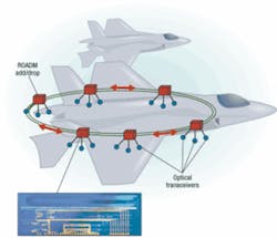
Designers use the silicon substrate to integrate unpackaged optical components such as lasers, photodiodes, and micro-optic elements in die form onto one chip and then package the chip in one package. Precisely micromachined features in the substrate permit automatic alignment and attachment of different components - all accurate enough for reliable communications between them.
The optical communications between components on the PLC chip and between a variety of optical functions flow over integrated optics. The optical waveguides are fabricated in glass films deposited on silicon - so-called silica-on-silicon technology. The majority of optical functions, such as splitters, tunable filters, polarizers, multiplexers and demultiplexers are developed and implemented today on PLC via monolithic integration. The combination of the packaging and integrated optics aspects of PLC technology makes it an attractive and powerful technology.
Use of silicon wafers draws extensively on the mass-production techniques of the commercial IC world, because the fabrication of PLC chips uses many of the same pieces of equipment and processes. The net result is the integration of sophisticated and multi-element photonic sub-systems into mass-produced PLCs.
For defense engineers, perhaps the most exciting fact about PLCs is their influence on size and weight. Freeing each of the components from their individual hermetic package results in 10 times or more reduction in subsystem size and weight. Eliminating excess packaging, of course, also reduces the likelihood of subsystem failure because of interconnect failure.
Flexible amplifiers
A second major improvement in photonics has come in amplification. Previously only electronics permitted amplification of the signal at any location in the IC circuit. In optics, by contrast, the conventional discrete erbium-doped fiber amplifiers (EDFAs) are bulky and impractical for insertion into optical modules. Yet the erbium-doped waveguide amplifiers (EDWAs) that replace EDFAs are small and flexible enough to fit anywhere on the PLC chip. This is a major advance. No longer do designers of optical subsystems have to calculate a “loss budget.” Instead, they can insert small, unpackaged gain elements anywhere on the device, thus creating a true lossless circuit equal to any counterpart in electronics.
This new capability opens vast opportunities for design flexibility and easy upgrade. Adaptation to altered circumstances, once nearly impossible, now becomes practical and achievable. Communications-link designers will now be able, for example, to insert lossless add/drop nodes or more bandwidth as necessary, whatever the platform or whatever the degree of upgrade required.
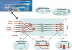
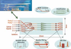
The current capabilities of optoelectronic integration are illustrated in Figure 1. In this figure a four-amplifier array is integrated on one chip. More than 30 optical elements are integrated here. The blue rectangule represents a silicon chip of 25 by 9 millimeters. The functions of individual elements on the chip are illustrated. “On-the-chip” photodiodes monitor the input and output signals, and adjust the pump intensity via variable optical attenuators that control each amplifier independently. The pump and signal combine via integrated-wavelength-selective multiplexers. An integrated filter eliminates the residual pump. The four amplifiers share two pumps, thereby reducing power consumption and cost.
Tunability
In the past five years, tunable optics has become commercial and practical. Just as electronics has long permitted users to tune at will to different radio or microwave frequencies, now optics makes it equally possible to tune to different wavelengths of light. Now logistics planners, instead of transporting an inventory of 40 separate laser and filter replacements, need only provision one type each.
Taken together, each of these advances has created a new generation of optical components that opens opportunities for bold, new defense system design. In addition to communications systems, new possibilities are emerging for military sensors, such as very precise gyroscopes, environmental sensors, and imaging sensors.
Navigation systems are becoming more and more prevalent in the “smart weapons” ranging from cruise missiles and to laser-guided bombs. The efficiency of these weapons has been clearly demonstrated in recent conflicts, and reliance on them will only increase. A typical navigation unit has a three-axis gyro and accelerometers to identify the position and velocity of the object in space at any given moment. The new photonics is leading the way in upgrading these systems, replacing old mechanical and optical devices that cannot satisfy weight, volume, and cost requirements
Consider, for example, the fiber-optic gyro (FOG) - a mature technology that has mostly found applications in the upper end of navigation applications. With the advent of PLC integration, FOGs are becoming feasible in a much broader range of applications. The PLC technology integrates the majority of discrete components currently used in the gyro, reducing size, weight, and cost.
Similarly, an important application of sensors is in UAVs, where performance has suffered from focusing so narrowly on their mission that the aircraft fail to sense what is going on around them. This influences the survivability and reconfigurability of the UAV.
Smart skins
To correct that deficiency, designers are looking at fiber-optic-based, smart skins that could recognize targets and enemy threats. Smart skins also could recognize the signatures of friendly UAVs and help coordinate joint maneuvers - swarming away from an oncoming missile or cooperatively engaging a target.
Such rapid-response intelligence, of course, requires large amounts of information at high speeds. The smart-skin approach would require sensors to detect RF energy and then modulate the signals via optical interconnects back to a central processor. In essence the platform skin would become one multi-element antenna/receiver consisting of a polymer/mylar mesh grid of interlaced waveguides connected to sensor interfaces. The grid would be so interconnected and reconfigurable that damage from an enemy bullet could not disrupt overall data gathering and processing.
Similar meshes found use in earlier designs such as the one for temperature and pressure monitoring on hydrogen and oxygen fuel tanks on the now-cancelled X-33 spacecraft prototype. Those projects required customized design and assembly, including hundreds of fiber-Bragg-grating devices connected by fiber-optic cabling, each handling a slightly different wavelength. By contrast, a smart skin could be readily manufacturable and might actually come on a roll - like contact paper. It could be applied to the UAV by rolling it out, laying it on the wings, and connecting it to multiple transceivers arrays.
Although the final design of such smart skins is by no means complete, it is clear that post-telecom-bubble optical components - PLCs, amplifiers, tunable lasers, etc. - will provide the underlying technology that makes it all possible. In essence, the components will comprise a low-cost, compact interface between sensors, the optical network, and the electronic signal processors controlling the flight.
Work yet to be done
Two other related steps are necessary before the new photonics can realize its potential in military platforms.
The first is the need to ruggedize virtually all commercial system elements for use under military conditions. For example, in-flight temperature variations will range far wider than the standard telecommunications range of -40 to 85 degrees Celsius. We will need to alter the optical component circuitry and make modifications necessary for it to operate efficiently such as turning off thermal shutdowns. And we will need to protect components further by putting them in environmentally protected device enclosures.
Second, we need to make these technologies easier for service personnel to live with in the field. Aircraft maintenance crews, for example, are used to handling copper cables. Copper is forgiving, but current commercial optical fiber is not. However, bend-resistant fiber does exist that could help make a fiber-optic cable rugged enough for many military applications.
Similarly, service personnel often clean dirty copper cable with spit-and-rag techniques, but are surprised when the same technique does not work for fiber. Designers are looking at different kinds of connecters that are not so sensitive. Core technology, no matter how powerful, almost always has to come down to earth to be truly useful.
In-the-field diagnostics also needs work. If something breaks, service personnel need to be able to figure out what is wrong and how to fix it. Designers are looking at, among other approaches, embedded loop-back and embedded optical time domain reflectometry (OTDR)-type capabilities.
All these field problems require solutions before we can realize the potential of the core technology, yet the fact that many of us have begun to concentrate on them can also be taken as a good sign. The broad use of photonics in military applications is emerging and will continue to expand in the near term as the performance weight, volume, fault tolerance, and scalability benefits of optical communications and sensors become known and the issues regarding their reliable operation in severe military environments are addressed.
Rick Stevens is Chairman of the Lockheed Martin Corporate Photonics Technology Focus Group. Joseph Shmulovich, is cofounder and executive vice president of engineering at Inplane Photonics in South Plainfield, N.J.


