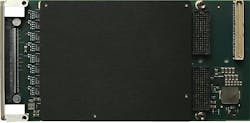
XMC embedded computing module with 24 A/D converter input channels introduced by TEWS Technologies
HALSTENBEK, Germany – TEWS Technologies in Halstenbek, Germany, is introducing the TXMC638 standard single-width Switched Mezzanine Card (XMC) embedded computing module to provide a user-configurable Kintex-7 field-programmable gate array (FPGA) with 24 A/D converter input channels.
Designed for industrial, COTS, and transportation applications, where specialized I/O or long-term availability is required, the TXMC638 provides a customizable interface for unique applications and a FPGA-based design for long-term product life cycle management.
The TXMC638 A/D converter input channels are based on the Linear Dual 16-Bit 5-megasample-per-second differential LTC2323-16 A/D converters. Each of the 24 channels has 16-bit resolution and works as quickly as 5 megasamples per second.
The analog input circuit is designed to allow input voltages to plus-or-minus 2.5 volts on each input-pin resulting in a plus-or-minus 5-volt differential voltage range.
For customer-specific I/O extension or inter-board communication, the TXMC638 provides 64 I/Os on P14 and 4 multi-gigabit-transceiver on P16. The P14 I/O lines are connected to the FPGA and can be used as 64 single ended LVCMOS24 or as 32 differential LVDS25 interfaces. Additionally, the TXMC638 provides three 100 Ohm terminated ac-coupled, differential inputs with wide input voltage range.
Related: 32 bit PMC for aerospace, defense, and transportation introduced by TEWS Technologies
All front I/O lines such as the A/D converter interface and the three 100 Ohm inputs are connected to a 98-pin Samtec ERF8-049 rugged EdgeRate connector. A 1-gigabyte, 32 bit wide DDR3 SDRAM is connected to the user FPGA. The SDRAM-Interface uses an internal Memory Controller of the Kintex-7.
The user FPGA is configured by a serial SPI flash. For full PCIe specification compliance, the XILINX Tandem Configuration Feature can be used for FPGA configuration.
XILINX Tandem Methodologies "Tandem PROM" is the favored methodology. The SPI flash device is in-system programmable. An in-circuit debugging option is available via a JTAG header for read back and real-time debugging of the FPGA design (using Xilinx "ChipScope").
For more information contact TEWS Technologies online at www.tews.com.
Learn more: search the Aerospace & Defense Buyer's Guide for companies, new products, press releases, and videos

