Design and development tool to help circuit board designers optimize design variables introduced by Samtec
NEW ALBANY, Ind. – Samtec Inc. in New Albany, Ind., is introducing the Signal Integrity Breakout Region Guru (SIBORG) tool free of charge to enable circuit board designers to optimize their product launches.
Available free to Samtec customers under NDA, SIBORG works with Ansys HFSS 3D Layout to generate, visualize, optimize, and develop printed circuit board package and component break-out regions.
Initially intended for use during design collaboration, the tool also helps users analyze different design variations rapidly in the connector breakout region that affect signal integrity.
The tool helps users adjust circuit board manufacturing design variables; backdrill drill size; BGA pad geometry; via geometry variables; antipad sizing variables; trace geometry variables; launch geometry variables; and break-out region array generation variables.
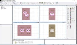
The SIbreak-out regionG tool has drop-down menus to specify design parameters and generates images to help set up, visualize, and analyze the effects of changing the variables.
After optimizing the design, results and s-parameters can transfer to other tools for end-to-end channel simulation. Designers also can export the final design into a module of circuit board break-out regions and package and connector 3D models.
Those interested can request the Signal Integrity Break Out Region Guru modeling tool through the Samtec website at www.samtec.com/hfss. For more information contact Samtec online at www.samtec.com.

