Shorten Design Cycles And Minimize Risk; Getting The Most Out Of The Zynq UltraScale+ RFSoCs
When confronted with a project schedule, when was the last time you heard “take as long as you need” or “if it doesn’t work the first time, don’t worry, you can always spin the design again”? Probably never. As FPGAs become more and more powerful and the scope of processing tasks becomes larger, shortening design cycles and minimizing risk has never been more critical.
Pentek, as a manufacturer of Commercial Off the Shelf (COTS) FPGA-based data processing and acquisition products, is often the interface between FPGA technology and the end user’s application. This puts Pentek in the unique position of supporting the customers as engineering partners with the ultimate shared goal of solving their end requirements. Pentek has learned a lot about how to shorten design cycles and minimize risk for the customers. Below is a short list of strategies that Pentek, and their customers, have found valuable.
Leverage FPGA Design Tools
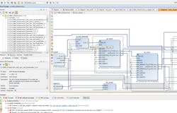
Every Pentek FPGA-based product ships with a complete set of functions installed as IP. While the products can be used as out-of-the-box solutions for data acquisition and processing, most customers will install their own custom IP for application-specific processing. The Pentek Navigator FPGA Design Kit used with the Zynq® UltraScale+™ RFSoC includes all of the factory installed IP as well as a library of general-purpose IP that can be used as building blocks for user applications. The library is provided as IP Integrator blocks, allowing the design to be easily imported into Xilinx’s Vivado® Design Suite. All blocks are defined using AXI4 and are designed to work seamlessly with Xilinx provided IP. This allows immediate access to the design, eliminating the need to learn any new tools or IP design definitions, saving startup time.
Utilize Factory-Provided IP Functions
While every customer’s design is different, many of the functions needed for those designs are similar. The IP provided with each hardware product not only supports the features of the hardware, like data acquisition blocks for A/D converter boards and waveform generator blocks for D/A converter boards, but also supports high-level functions that are most common for the types of applications typically addressed by the hardware. For example, the Pentek products that use Zynq UltraScale+ RFSoCs are supported with a library of functions including:
- Data acquisition for capturing and streaming A/D data
- Waveform generation for streaming data to the D/A or playing back waveforms stored in memory
- A radar chirp and signal generator for radar and test applications
- A/D calibrations functions
- 100GigE UDP engines
- DMA engines designed for high-speed data streaming
In each case, these IP functions can be used unaltered or modified by the user by editing the supplied VHDL source. In all cases, starting with competing, tested IP speeds up the development time and reduces risk.
Streamline the Path from Development to Deployment
Pentek’s Quartz family, which uses Zynq UltraScale+ RFSoCs, are all based on QuartzXM, a compact system on module containing the all the circuitry needed to support the Zynq UltraScale+ RFSoC.
The idea behind this design was simple: to address the most challenging aspects of PCB and circuit design in the module and guarantee the best possible analog and digital performance from the Zynq UltraScale+ RFSoC. With the module designed and proven, Pentek can offer the module on various carriers to support common form factors like PCIe® and 3U VPX.
While offering this design in standard form factors is important, the biggest benefit can be seen by customers who need to deploy Zynq UltraScale+ RFSoCs in space-restricted environments or in applications that cannot be satisfied with standard form factors. Pentek enables customers to design their own carrier for the QuartzXM by providing a design kit containing all of the electrical, mechanical, and thermal design information needed. By encapsulating so much of the critical design in the QuartzXM, the customer can start with a proven Zynq UltraScale+ RFSoC platform and concentrate on the simpler carrier design. It also provides a path for developing and prototyping on a standard, low-cost and readily available workstation like a desktop PC using the PCIe version of Quartz, or in the case of 3U VPX, in a low-cost Model 8257 development chassis. After the application IP and software are developed, the solution can then be migrated to the deployed system by designing the custom carrier when needed. Because the core hardware is the same in both systems, the IP and software can be moved from the development to the deployed system with no changes. All of these design techniques greatly reduce risk and shortens development time.
Engineer-to -Engineer Support Ensures Success for a Lifetime
Even with the best product documentation available, often a short engineer-to-engineer phone conversation can be the best tool to minimize risk and save time later in the design cycle. All Pentek products come with free, life-time support. Pentek customers can always reach an engineer if a problem does arise.
Design cycle time and risk mitigation are a very real part of the engineering process. And while risk will always be an inherent part of the process of inventing, Pentek continues to see mitigating that risk and shortening design cycle time as just as important as offering the highest performance and innovative products to the customers.
To learn more about Zynq UltraScale+ RFSoC, visit www.xilinx.com/rfsoc
To learn more about Pentek Quartz family, visit https://www.pentek.com/RFSoC/RFSOCPrd.cfm
To try out Pentek Navigator FPGA design kit, visit https://www.pentek.com/navigator/navigator.cfm


