Electronic design automation: Tool vendors chase escalating board design requirements
By John H. Mayer
Printed circuit board designers look to EDA tool providers to help them deal with a growing number of problems brought about by the shrinking sizes of circuits and interconnects.
For printed circuit board (PCB) design tool developers, the race to keep up with ongoing advances in component and subsystem design shows little sign of slowing down. As IC manufacturers drive down the process path well into deep sub-quarter micron territory, they are igniting a revolution in device capability. Mainstream microprocessors now run at gigahertz clock rates. Custom application-specific integrated circuits (ASICs) and field-programmable gate arrays (FPGAs) commonly pack millions of transistors and tremendous functionality into a tiny footprint. And chip packaging continues to venture into entire new territory as lead counts on high-density devices push well past 1,000 pins.
The impact on board designers has been daunting. "Over the last five or six years, we've seen a continual pressure to get more processing power into a given volume," notes Bill Scott, principle engineer with Sky Computers Inc. in Chelmsford, Mass. "It has forced us to pack more and more logic on a given size board and at the same time run whatever components we are able to fit on that board at higher and higher clock rates."
The latest version of the Sky Computers Merlin board is a stark example of that trend. Designed for compute-intensive applications in radar, signals intelligence, and weapon systems, the multiprocessor board packs 16 billion floating point operations per second (GFLOPS) of performance in a 6-by-6-inch square circuit card. Among the many high-performance components packed into the Merlin are four 500 MHz MPC7410 PowerPC microprocessors.
But increasingly high clock rates and dense board configurations are only part of the problem board designers face today. The latest advances in IC fabrication technology have also spawned devices with shorter and shorter edge rates. Whereas a few years ago high-speed components typically featured rise and fall times in the multi-nanosecond range, today comparable devices manufactured in deep sub-micron processes feature edge rates in the hundreds of picoseconds.
"Much of the silicon that comes out these days has very fast drivers and receivers and even if your design is not really what you would describe as a very high-speed design, the components are very high speed," notes Jamie Metcalfe, vice president of marketing for the Cadence PCB Division in Chelmsford, Mass.
The culmination of all these trends — higher clock rates, higher density routing requirements, and shorter edge rates — on signal quality can be devastating. Rapidly shrinking timing margins force designers to carefully consider delays caused by interconnects. Higher density routing requirements and faster edge rates create transmission line effects that can quickly lead to ringing, overshoot, and undershoot. And issues such as crosstalk and EMI suddenly become a serious obstacle to board reliability.
The problem, note tool vendors, is not the emergence of high-speed issues. Designers building systems for high performance military and aerospace applications have grappled with these issues for many years. It is the growing pervasiveness of the problem.
"If only five percent of your signals are high-speed constrained and you're building a board with 5,000 signals on it, that's only 250 nets and you can deal with that the way designers have traditionally approached the problem in a fairly manual way," Metcalfe explains. In a typical scenario, the engineer or signal integrity expert will sit next to the layout engineer and guide him or her through the layout to satisfy timing constraints and signal quality.
The problem comes when the percentage of nets facing these high-speed issues grows dramatically. "It's not uncommon today to see boards with 50 percent of the nets constrained in some way, and for those designers working on high-end military designs, it can often run to 80 or 90 percent," he says. "Suddenly that's a different problem that needs solving because it would take forever to walk net-by-net through the layout with the signal integrity engineer."
Tool vendors are helping board designers cope with this escalating problem by preaching the merits of verification. "It's something that designers have typically considered as an option but that game is changing," observes David Wiens, product marketing manager for PCB design products at Mentor Graphics Corp. in Wilsonville, Ore. "It's changing with timing, its changing with signal integrity, and it's even changing with issues that have been around for along time such as thermal analysis."
Moreover, shrinking time-to-market windows virtually demand that consideration of issues such as signal integrity analysis be moved up earlier in the design cycle. The days when a board design could lay out a board, build a prototype, and throw it over to a signal integrity expert to resolve outstanding signal quality issues are quickly disappearing. Once a problem is found at that late stage, the only option is to rebuild the board.
That is no way to meet time-to-market goals say tool vendors. "Anyone who delays SI analysis until the prototype stage runs a high risk of extending their design cycles and thereby jeopardizing the on-time delivery of their systems," says John Dube, engineering manager for Innoveda Inc. of Marlboro, Mass.
The key to identifying these potential problems and resolving them without re-spinning a board design is to perform analysis before layout, say tool vendors. Once designers can identify problems with signal integrity, electromagnetic compatibility (EMC) and crosstalk, they can constrain routing and stackup, define clock routing topologies, choose specific device speeds, and specify the net terminations they need to guarantee the design will be right first time.
If board designers are going to move verification up in the design cycle, however, they will need tools that are not only tightly integrated into the overall design environment, but also highly capable and easy to use.
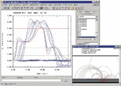
For tool vendors, these issues are a continuing work-in-progress. In late August, for instance, Mentor Graphics released new versions of the Tau-board level timing verification tool and ICX interconnect synthesis design and verification environment to address some of these concerns.
The latest version of Tau adds several ease-of-use enhancements for model creation and analysis. It allows users to import industry standard Timing Design Mark-up Language (TDML) files as part of the model creation process and provides additional information to users during analysis via graphical block diagram views as well as test-output files to simplify troubleshooting.
The latest version of ICX adds new simulation controls to give users greater flexibility during analysis. It also adds support for definition and routing of advanced topologies to give designers more options when solving signal integrity and timing problems during the physical implementation of the design.
Other tool vendors have made similar advances. The latest version of Cadence's PCB design environment includes new timing-path oriented interconnect topology rules that allows the designer to more easily design and simulate a constraint in SPECCTRAQuest SI Expert and then implement it with Cadence's Allegro layout tool and SPECCTRA autorouter. And in January Innoveda extended the capabilities of its XTK signal integrity analysis tool by adding SPICE co-simulation. The new capability allows designers to perform crosstalk analysis inside of dense IC packages and connectors.
Managing constraintsThe key to ensuring signal quality and maintaining tight timing margins once analysis is done is constraint-driven design. But as design complexity has risen, so, too, has the job of building and maintaining a board's electrical constraints."For example, in a single net you could specify a maximum delay for the signal to get to from the source to the last load on the net," Metcalfe says. "But within a single topology there are many different kinds of constraints you could introduce related to delay, length, overshoot, undershoot, crosstalk, and other issues. If you associate 40 or 50 different types of constraints with a topology and multiply that by hundreds or thousands of nets across a board design, it's easy to see the complexity of the problem."
The big issue, Metcalfe notes, is how the designer captures all of that information and communicates it to PCB layout. Moreover, how does he verify that the constraints were met and how is the information organized and stored so that designers on future projects can reuse the data.
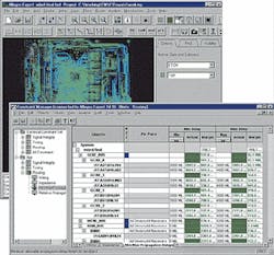
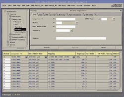
To help designers cope with that problem, Cadence has introduced a new constraint manager for PCB design. The new tool manages the process by providing a spreadsheet interface to design rules and combining it with a hierarchical view of electrical constraints contained in Allegro layout and Concept HDL schematic databases. The tool lets designers group high-speed constraints for a collection of signals into an electrical constraint set, which is then associated with their nets. Once the constraints are in the database, they are used to drive the placement and routing process for those signals.
The manager is integrated with Allegro's design rule checking system and the SPECCTRAQuest Signal Integrity Expert. That allows designers to check different high-speed rules in real time as the design process progresses. Results are presented in the constraint manager's spreadsheets. Any design parameters that violate their associated constraints are highlighted.
In the meantime, PCB tool vendors are continuing to evolve their rule-driven capabilities. In the latest version of its Hot-Stage virtual prototyping environment, for example, Zuken Ltd. in Westford, Mass., has added extensive new constraint-driven capabilities including a separate spreadsheet-based constraints manager, an automatic constraints wizard, a "what-if" editor that can be used up-front in the design process as a virtual scratchpad, and built-in analysis capabilities. Users of Hot-Stage 4 enter constraints and the tool synthesizes the design to meet requirements. A tree browser supports design navigation and a spreadsheet allows the user to edit electrical constraints. Violations are displayed in the same interface.
One of the more formidable challenges facing users of constraint-based design systems is the growing introduction of extremely high pin-count devices. "They're a designer's worst nightmare," says Mentor's Wiens. "The pins are in such a high density that you often have to sacrifice normal design rules to meet the unique demands of the package."
What designers need, Wiens argues, is the capability to combine automatic routing to a defined set of rules on much of a board and interactive or manual routing for these defined spaces. To meet this growing requirement, many tool vendors are adding new manual or editing capabilities to their design environments. Mentor, for instance, has recently added AutoActive technology, an approach the combines the power of shaped-based automatic routing with interactive editing. With it the board designer can define rules by area.
"If you have two different tools, you probably have different rules constraining them and you have to pass data back and forth," Wiens says. "This allows us to have the same rule set for both automatic and interactive editing and it helps shorten the design process."
Collaborating on design intentThe increasing complexity of board designs and the escalating need to push board verification and analysis up earlier in the design cycle has driven PCB tool developers to reconsider the types of solutions they supply today. Facing relentless time-to-market pressure, development teams must resolve a long list of issues from architectural and technology decisions, and resolving form, fit, and function questions to identifying component availability and cost issues and scheduling multiple tasks.How can development environments help product developers coordinate the many tasks that go into the building of a complex board solution? And how can a company's tool set support and simplify the collaboration and communication not only within engineering but also across the many functional groups in any organization?
"The products board designers are building today are so complex, they require design tools which enable collaboration beyond just engineering," says Innoveda's Dube. "They demand that design intent be communicated early in the design process so that design information and component choices can be shared with purchasing and manufacturing to ensure that the product can be built on schedule once the design is complete."
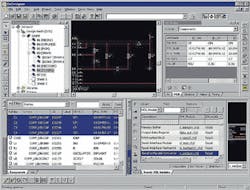
In May Innoveda announced a new web-based solution designed to knock down many of the traditional obstacles associated with a serial, step-by-step approach to board development. Called DxDesigner, the new design environment functions as a gateway between computer-aided engineering and team-based design collaboration. In essence Innoveda's product developers took their existing front-end products, enhanced many of them, and then tightly bundled them together to help designers tackle the complexity of integrating subsystems, minimize the time spent in researching and selecting components, and track down the signal performance problems associated with high-speed devices.
"What we're really trying to do here is look at the whole front end of design in a different way," Dube explains. "Instead of having individual point tools for all sorts of things, we're doing something called design definition."
This new concept combines four basic process technologies — component information systems, design entry and sharing, simulation and planning, and enterprise connectivity — within a one integrated suite of tools and services. Within it, designers can more easily reuse existing components or subsystems, find and resolve signal integrity issues, develop physical constraints based on that analysis, and in the process minimize design iterations and shorten the design cycle. Moreover, it allows geographically dispersed teams to coordinate their efforts and minimize redundancy through the use a centralized, approved parts library.
Innoveda is offering DxDesigner in three different configurations. The basic configuration provides a hierarchical tree view of the design and adds a navigator to display components and nets for a given design context, a multi-object attribute editor, a design drawing tool, a parts and design selection tool, and a design synchronization capability that manages design data.
To help engineers collaborate on design intent, the environment enables users to see schematics through a web-based viewer over the Internet. The second configuration DxDesigner EE builds off the original configuration and adds analog, digital or mixed analog-to-digital design, and simulation capabilities. DxDesigner HSD moves a step further by adding high-speed PCB planning capabilities including a graphical pre-placement tool to define and analyze critical component selections, a spreadsheet for entering and managing constraints, a graphical tool for designing and simulating net topologies using Innoveda's XTK simulation engine, and an analysis tool capable of sweeping high-speed parameters to determine constraints for placement and routing.
One of the driving forces behind new collaborative design environments like DxDesigner is the increasing need to link the designer to key component information. By some estimates board designers spend as much as 30 percent of their time researching and selecting parts. The inordinate amount of time spent on this task often reflects the inability of designers to quickly and simply access supply chain data.
Moreover, information on parts availability and status is constantly changing. In most organizations the transfer of parts information between a parts supplier and the board designer travels through the purchasing department, often manually, and the potential for delayed or inaccurate communication is high. It is crucial that designers have access to this data as early as possible in the design cycle to avoid designing in an obsolete part or driving up end product cost to unacceptable levels.
DxDesigner solves this problem by adding interfaces to Agile and MatrixOne, two tools that allow the engineer to generate a bill-of-materials (BOM), input it into existing component inventories, and verify it for accuracy. This capability allows the engineer to distribute design data to other groups in the enterprise such as manufacturing and procurement and helps ensure that the design group has the latest information on parts approval and availability.
"It is becoming increasingly clear that the more component data the designer has early on the design process, the more time he saves downstream," Wiens agrees. In July Mentor Graphics introduced DMS2000.5, a data management system designed to incorporate supply chain information into the design process. Using an object-oriented relational technology called DataFusion, the new tool consolidates and manages data from multiple sources and of multiple types including component information, component quality information, component supply information, ECAD libraries, documentation, and BOM release data. It interfaces with EDA design tools from Mentor, Cadence and Zuken.
Mentor is offering DMS2000.5 in two configurations. A workgroup version is designed for mid-sized design teams and is configurable for quick deployment. DMS Enterprise supports larger organizations including global design teams.
Maximizing reuseAnother key step to increasing board designer's productivity is maximizing the reuse of proven components. This concept now extends well beyond the reuse of a single component. It can include a block of logic and the constraints and topologies used to define it. Or it can include a module as large as an entire board.The concept of design reuse is hardly new, but the implementation has never been easy. "Designers have been employing design reuse concepts for years, but it has traditionally been a manual process," Metcalfe notes.
To facilitate this process Cadence has upgraded its PCB design environment to support a team-based approach to modular design reuse. The latest version of Cadence's Allegro layout tool adds database-driven design reuse capabilities, which let the designer create or define modules that can consist of the logical schematic and the physically implemented PCB layout. These modules can now be stored as a reusable library element and accessed by other designers. The user simply specifies that the module is to be used in future designs before netlisting and promoting it to a reference library. Allegro automatically senses a netlist containing reuse modules and pulls in the physical representation stored in the reference library.
Power issuesDeveloping reliable power delivery schemes is another growing issue in high-performance PCB design. Over the past decade the power requirements in processor-based systems have continually escalated even as designers have moved to lower-voltage suppliers."Back in the early 1990s power requirements generally ranged somewhere between 5 to 10 watts," notes Hemant Shah, product marketing director for SPECCTRAQuest at Cadence Design Systems. "Today many advanced processor-based systems need over 100W of power so even those voltage requirements have gone down, current requirements have gone up."
This trend has had a significant impact on product reliability. Power delivery systems must now be able to supply power at a wide range of frequencies explains Shah. If the designer does not take that precaution, the behavior of high-speed components becomes very unpredictable and a simple code sequence could initiate a systems crash. "The slightest ripple can cause the system to fail," he notes.
Early on, board developers tried to solve this problem by over designing their systems. "What designers tended to do is throw in a lot of decoupling capacitors around the chips requiring high current," says Shah. "They knew they had a problem and didn't have a tool to solve it, so they took this approach and hoped for the best."
Standalone simulation tools offered an alternative solution. But they forced the designer to build the design, analyze it, run through "what-if" type scenarios, and then manually enter the design modifications back into the design tool in a time-consuming process. Moreover these tools were based on time-domain simulation when what was needed was a tool capable of frequency domain analysis to assure that over all the frequency ranges of interest, the power delivery system would deliver the right amount of current
Board designers at Sun Microsystems began to run into this problem about five years ago as they began to build system boards running at higher and higher clock rates. To solve the problem they developed their own frequency domain analysis tool. "Basically we developed an internal tool to perform this analysis ourselves and since we were already standardized on Cadence's Allegro and SPECCTRAQuest, we sort of hacked it into the Cadence toolset," explains John McGuigan, market development alliance manager at Sun.
After using it for a few years, Sun decided to license its technology to Cadence. Earlier this
year Cadence and Sun announced the availability of a new Power Integrity module for SPECCTRAQuest design and analysis tools from Cadence. "Licensing it gets the tool we developed professionally integrated into Cadence's whole tool suite so it makes it easier to use," he explains. "And it gets our engineers out of a support role."
Typically the tool is employed in a new board design after floor planning but before routing. The module blocks the board into a grid and plots impedance for each grid. This allows the designer to identify problem areas, select capacitors from an integrated component library, and work on the board from grid to grid to bring impedance levels down to specified targets. "You can choose a decoupling capacitor to solve a problem, simulate it and analyze the results immediately," Shah says.
Integrating the module into a comprehensive design environment and moving power delivery analysis up earlier has a significant impact on design cycle time. But it also dramatically cuts end product cost. "We've already seen instances where the number of capacitors used in a design have been reduced by half and that's a lot of dollars in a high-volume product," says Shah.
Integrating mechanical considerationsOne of the biggest obstacles to so-called "right-first-time" board design is the potential mismatch between electrical and mechanical design. The inability to simulate an electrical design in the context of substrates, enclosures, and other mechanical features of a design can easily result in wasted space, larger end-product footprint, and higher costs. Moreover, the exchange of data between the electrical and mechanical design groups can often lead to loss of data or inaccuracies generated during the ECO process. Typically the fewer times tool users have to manually intervene in the data transfer process, the fewer errors that occur."Every tool vendor has ties into mechanical systems, but they're still two separate systems right now," Wiens notes. "Clearly the development of a single system that can handle both will be ideal."
In the meantime, vendors continue to close the gap between mechanical and electrical design. To help eliminate time-consuming iterations between PCB and mechanical design groups, Zuken recently brought to market a new design tool that provides automatic verification of a PCB design in its 3D environment.
The tool, called EM Checker, allows users to load and model enclosure and obstacle information into the ECAD environment using the ISO-standard STEP AP203/AP214 format. It integrates directly into Zuken's design flow and, through the company's Companion Series Program, also integrates into any third-party PCB design flow that uses the industry standard CADIF format.
The tool not only reduces design time by forging a bridge between mechanical and electrical design, it also allows designers to build to smaller footprints. "With the designs we've seen, space savings can range from 10 to 20 percent or more depending on whether the design includes irregularly shaped or curved components or enclosures," says Duncan Hooper, senior technical officer for Zuken Ltd. in Bristol, England.
EM Checker gives the designer the ability to visually verify the PCB in its environment and supports views in wireframe, shaded or hidden-line-removal modes. "In shaded mode, for example, it is easy to visually check that no part of the electronics interferes with the enclosures," explains Hooper. The designer can also generate cutaway views to see inside an assembly. An integrated measurement tool provides calculations of the minimum distance between two 3D objects to ensure critical clearance checking.


